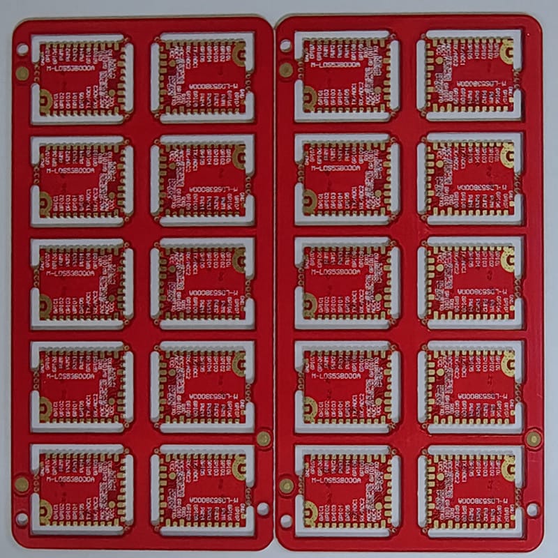
Prototype printed circuit boards RED solder mask castellated holes
Product Specification:
| Base Material: | FR4 TG140 |
| PCB Thickness: | 1.0+/-10% mm |
| Layer Count: | 4L |
| Copper Thickness: | 1/1/1/1 oz |
| Surface treatment: | ENIG 2U” |
| Solder mask: | Glossy red |
| Silkscreen: | White |
| Special process : | Pth half holes on edges |
Application
The processes of plated half holes are:
1. Process the half-side hole with double V-shaped cutting tool.
2. The second drill adds guide holes on the side of the hole, removes the copper skin in advance, reduces burrs, and uses groove cutters instead of drills to optimize the speed and drop speed.
3. Immerse copper to electroplate the substrate, so that a layer of copper is electroplated on the hole wall of the round hole on the edge of the board.
4. Production of the outer layer circuit after lamination, exposure, and development of the substrate in sequence, the substrate is subjected to secondary copper plating and tin plating, so that the copper layer on the hole wall of the round hole on the edge of the board is thickened and the copper layer is covered with covered by a tin layer for corrosion resistance;
5. Half-hole forming cut the round hole on the edge of the board in half to form a half-hole;
6. In the step of removing the film, the anti-electroplating film pressed during the film pressing process is removed;
7. Etching the substrate is etched, and the exposed copper on the outer layer of the substrate is removed by etching;
8. Tin stripping the substrate is stripped of tin, so that the tin on the half-hole wall can be removed, and the copper layer on the half-hole wall is exposed.
9. After forming, use red tape to stick the unit boards together, and remove the burrs through the alkaline etching line
10. After the second copper plating and tin plating on the substrate, the round hole on the edge of the board is cut in half to form a half hole, because the copper layer of the hole wall is covered with a tin layer, and the copper layer of the hole wall is completely intact with the copper layer of the outer layer of the substrate Connection, involving strong bonding force, can effectively prevent the copper layer on the hole wall from being pulled off or copper warping when cutting;
11. After the half-hole forming is completed, the film is removed and then etched, so that the copper surface will not be oxidized, effectively avoiding the occurrence of residual copper or even short circuit, and improving the yield rate of the metallized half-hole PCB circuit board.
FAQs
Plated half-hole or castellated-hole, is a stamp-shaped edge through cutting in half on the outline. Plated half-hole is a higher level of plated edges for printed circuit boards, which is usually used for board-to-board connections.
Via is used as an interconnection between copper layers on a PCB while the PTH is generally made larger than vias and is used as a plated hole for acceptance of component leads - such as non-SMT resistors, capacitors, and DIP package IC. PTH can also be used as holes for mechanical connection while vias may not.
The plating on the through holes is copper, a conductor, so it allows electrical conductivity to travel through the board. Non-plated through holes do not have conductivity, so if you use them, you can only have useful copper tracks on one side of the board.
There are 3 types of holes in a PCB, Plated Through Hole (PTH), Non-Plated Through Hole (NPTH) and Via Holes, these should not be confused with Slots or Cut-outs.
From IPC standard, it’s +/-0.08mm for pth, and +/-0.05mm for npth.
Products categories
-

Pcb processing prototype board 94v-0 Halogen-fr...
-

fast pcb prototyping service pcb prototype china
-

BYD Electric Vehicles PCB circuit board prototy...
-

Electric car prototype printed circuit board ma...
-

Halogen-free Automotive circuit board quick tur...
-

Consumer pcb fabrication 94v-0 circuit board di...