Pcb prototype pcb fabrication blue solder mask plated half-holes

Product Specification:
| Base Material: | FR4 TG140 |
| PCB Thickness: | 1.0+/-10% mm |
| Layer Count: | 2L |
| Copper Thickness: | 1/1 oz |
| Surface treatment: | ENIG 2U” |
| Solder mask: | Glossy blue |
| Silkscreen: | White |
| Special process : | Pth half holes on edges |
Application
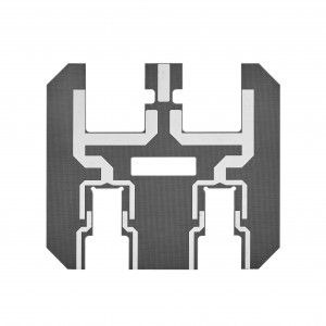
PCB half-hole board refers to the second drilling and shape process after the first hole is drilled, and finally half of the metallized hole is reserved. The purpose is to directly weld the edge of the hole to the main edge to save connectors and space, and often appear in signal circuits.
Half-hole circuit boards are usually used for mounting high-density electronic components, such as mobile devices, smart watches, medical equipment, audio and video equipment, etc. They enable higher circuit density and more connectivity options, making electronic devices smaller, lighter and more efficient.
The non-plated half hole on the edges of the PCB is one of the commonly used design elements in the PCB manufacturing process, and its main function is to fix the PCB. In the process of PCB board production, by leaving half holes at certain positions on the edge of the PCB board, the PCB board can be fixed on the device or the housing with screws. At the same time, during the PCB board assembly process, the half hole also helps to position and align the PCB board to ensure the accuracy and stability of the final product.
The half hole plated on the side of the circuit board is to improve the connection reliability of the side of the board. Usually, after the printed circuit board (PCB) is trimmed, the exposed copper layer at the edge will be exposed, which is prone to oxidation and corrosion. In order to solve this problem, the copper layer is often coated in the protective layer by electroplating the edge of the board into a half hole to improve its oxidation resistance and corrosion resistance, and it can also increase the welding area and improve the reliability of the connection.
In the process of processing, how to control the product quality after forming semi-metallized holes on the edge of the board, such as copper thorns on the hole wall, etc., has always been a difficult problem in the processing process. For this type of board with a whole row of semi-metallized holes The PCB board is characterized by a relatively small hole diameter, and is mostly used for the daughter board of the mother board. Through these holes, it is welded together with the mother board and the pins of the components. When soldering, it will lead to weak soldering, false soldering, and serious bridging short circuit between the two pins.
FAQs
It might be useful to place plated holes (PTH) on the board edge. For instance when you want to solder two PCB’s onto each other in a 90° angle or when soldering the PCB to a metal casing.
For example, the combination of complex microcontroler modules with common, individually designed PCBs. Additional applications are display, HF or ceramic modules which are soldered to the base printed circuit board.
Drilling- plated through hole (PTH) - panel plating - image transfer - pattern plating -pth half hole- striping - etching - solder mask - silkscreen - surface treatment.
1.Diameter ≥0.6MM;
2.The distance between hole edge ≥0.6MM;
3. The width of etching ring needs 0.25mm;
Half-hole is a special process. In order to ensure that there is copper in the hole, it must mill edge first before plating copper process. The general half-hole PCB is very small, so the cost of it is more expensive than the common PCB.