Our guiding principle is to respect the customer's original design while leveraging our production capabilities to create PCBs that fulfill the customer's specifications. Any changes to the original design require written approval from the customer. Upon receiving a production assignment, MI engineers meticulously examine all the documents and information provided by the customer. They also identify any discrepancies between the customer's data and our production capacities. It is crucial to fully comprehend the customer's design objectives and production requirements, ensuring all requirements are clearly defined and actionable.
Optimizing the customer's design involves various steps like designing the stack, adjusting the drilling size, expanding the copper lines, enlarging the solder mask window, modifying the characters on the window, and performing layout design. These modifications are made to align with both production needs and the customer's actual design data.
PCB production process
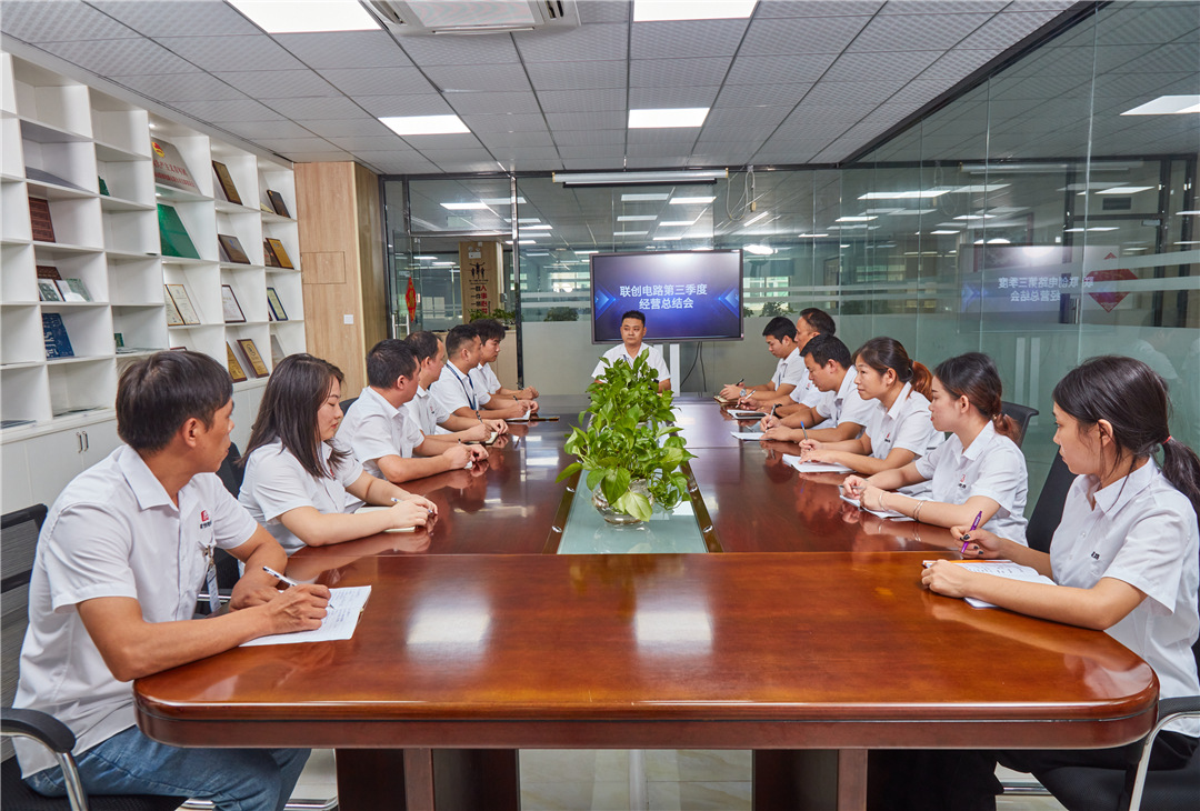
Meeting room
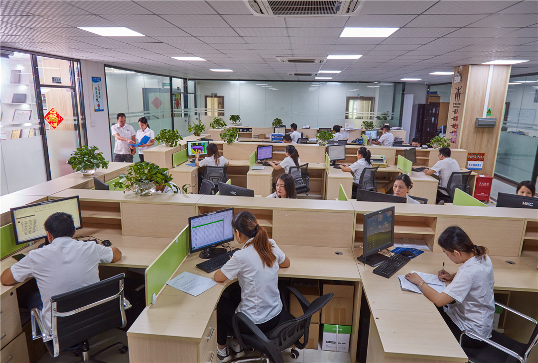
General office
The process of creating a PCB (Printed Circuit Board) can be broadly broken down into several steps, each involving a variety of manufacturing techniques. It's essential to note that the process varies depending on the structure of the board. The following steps outline the general process for a multi-layer PCB:
1. Cutting: This involves trimming the sheets to maximize utilization.
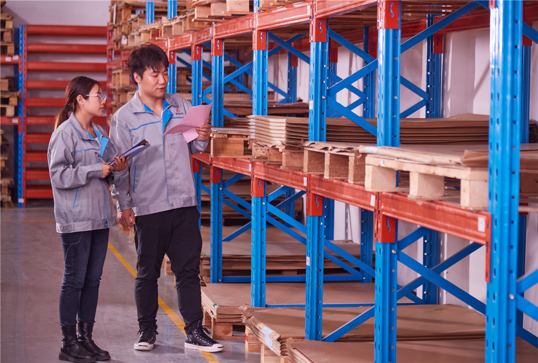
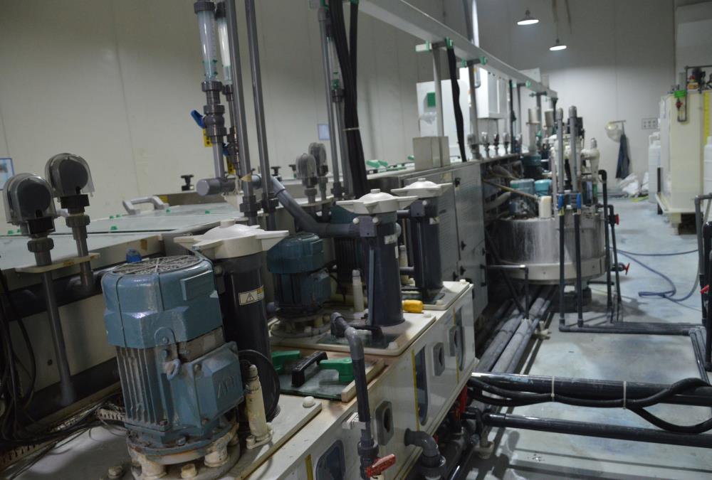
Material Warehouse
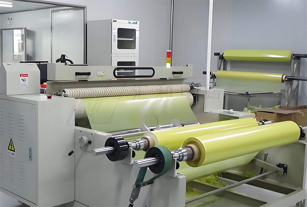
Prepreg Cutting Machines
2. Inner Layer Production: This step is primarily for creating the internal circuit of the PCB.
- Pre-treatment: This involves cleaning the PCB substrate surface and removing any surface contaminants.
- Lamination: Here, a dry film is adhered to the PCB substrate surface, preparing it for the subsequent image transfer.
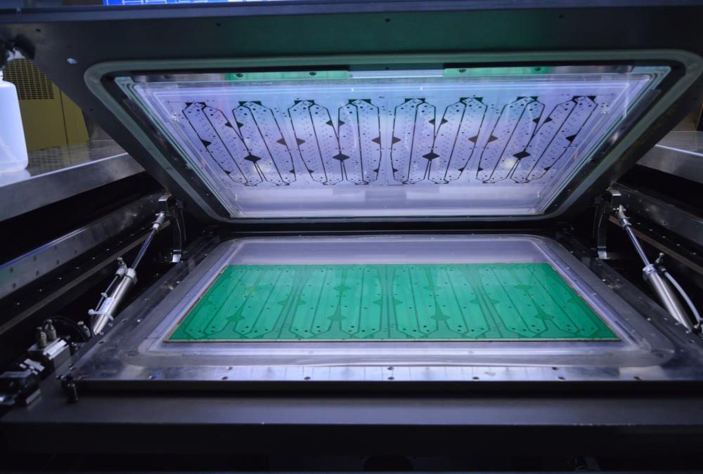
- Exposure: The coated substrate is exposed to ultraviolet light using specialized equipment, which transfers the substrate image to the dry film.
- The exposed substrate is then developed, etched, and the film is removed, completing the production of the inner layer board.
Edge planing machine
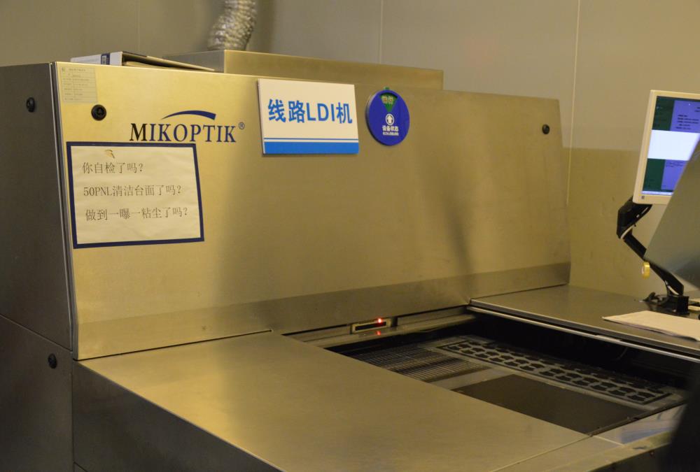
LDI
3. Internal Inspection: This step is primarily for testing and repairing the board circuits.
- AOI optical scanning is used to compare the PCB board image with the data of a good-quality board to identify defects such as gaps and dents in the board image. - Any defects detected by AOI are then repaired by the relevant personnel.
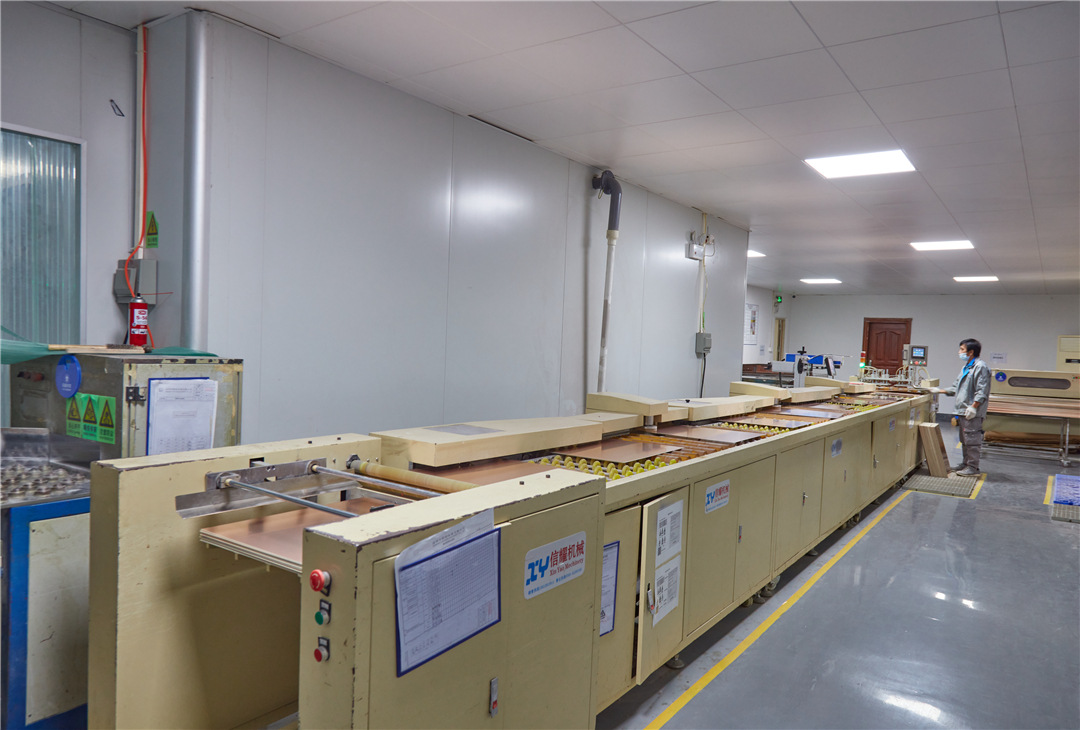
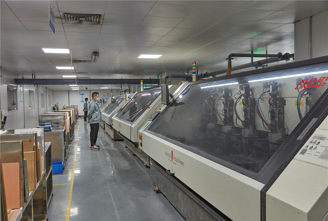
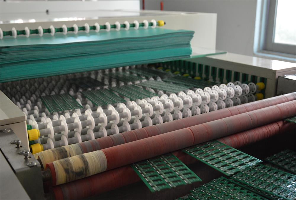
Automatic Laminating Machine
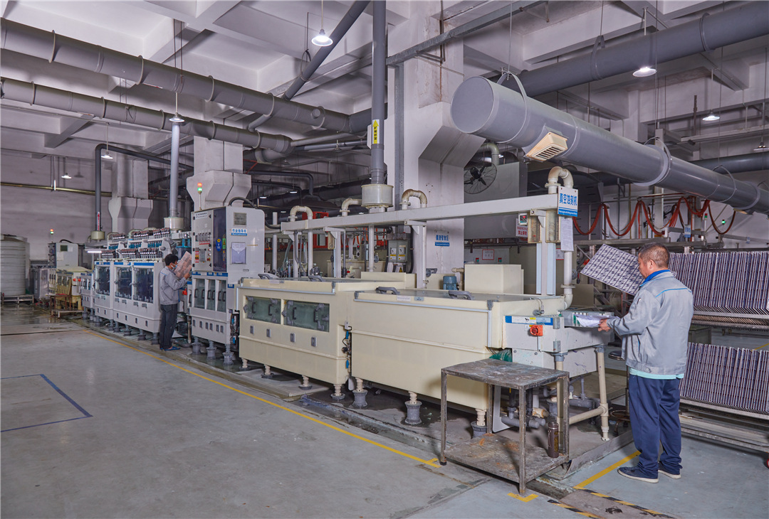
4. Lamination: The process of merging multiple inner layers into a single board.
- Browning: This step enhances the bond between the board and the resin and improves the copper surface's wettability.
- Riveting: This involves cutting the PP to a suitable size to combine the inner layer board with the corresponding PP.
- Heat Pressing: The layers are heat-pressed and solidified into a single unit.
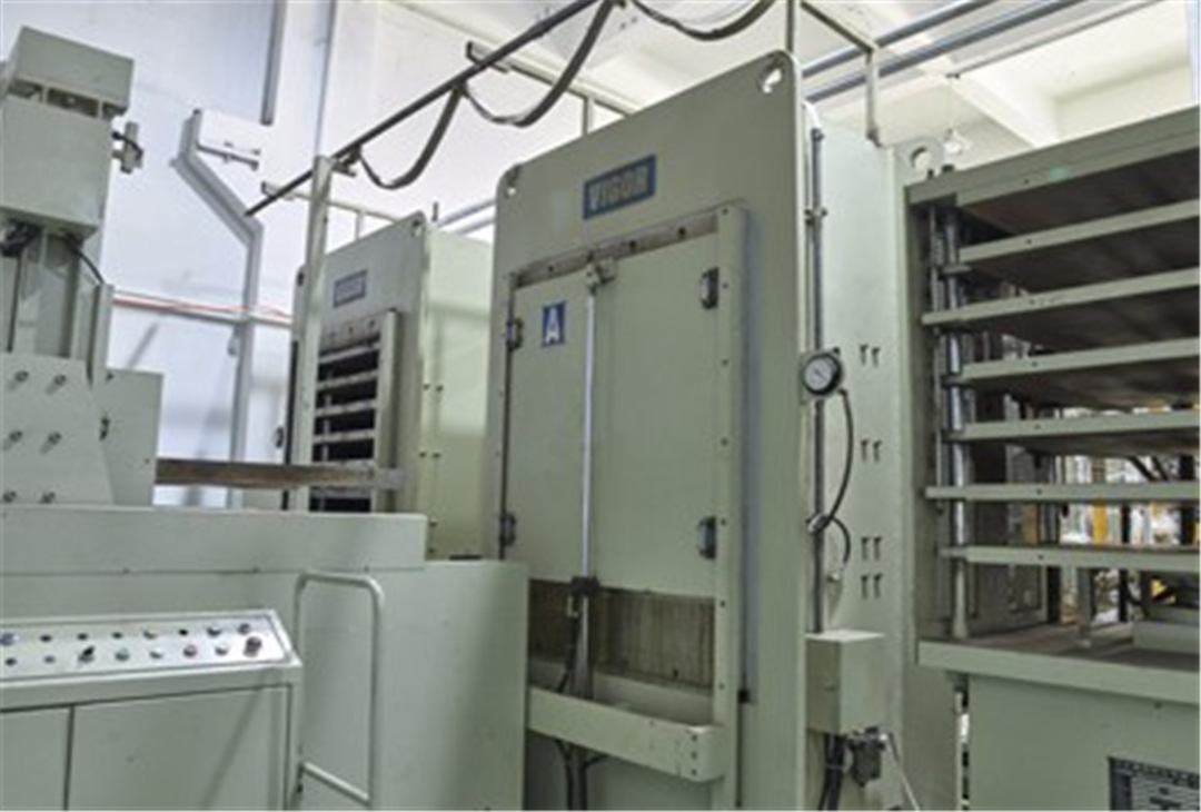
Vacuum hot press machine
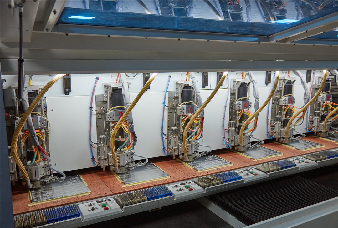
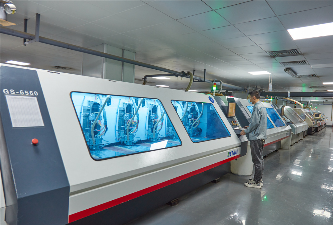
Drill machine
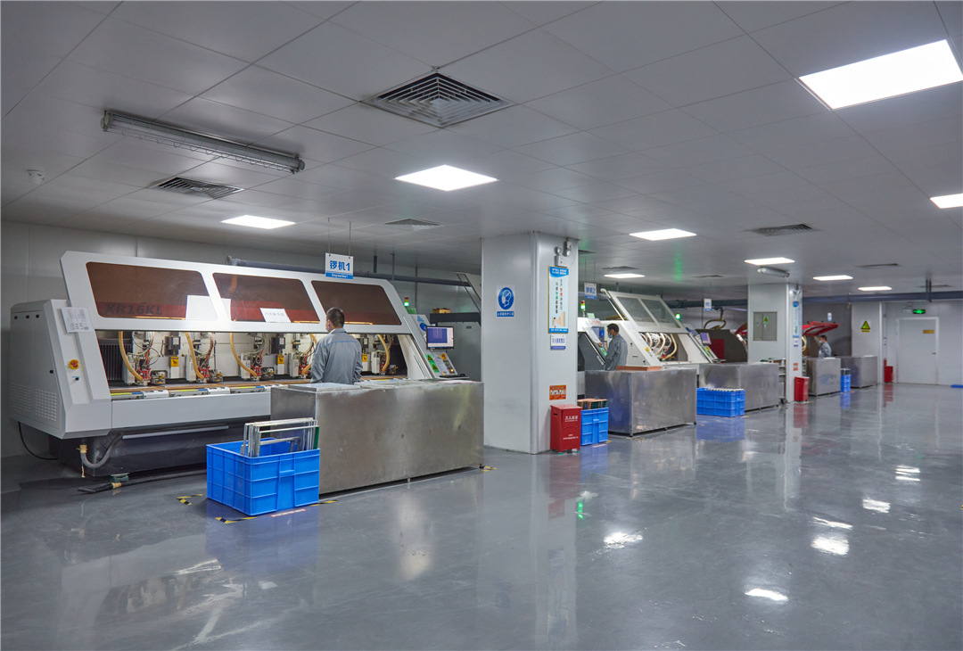
Drill Department
5. Drilling: A drilling machine is used to create holes of various diameters and sizes on the board as per customer specifications. These holes facilitate subsequent plugin processing and aid in heat dissipation from the board.
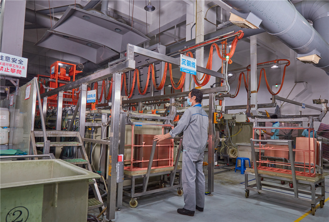
Automatic Sinking Copper Wire
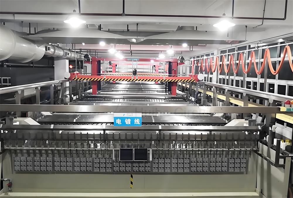
Automatic Plating Pattern Line
Vacuum etching machine
6. Primary Copper Plating: The holes drilled on the board are copper plated to ensure conductivity across all board layers.
- Deburring: This step involves removing burrs on the edges of the board hole to prevent poor copper plating.
- Glue Removal: Any glue residue inside the hole is removed to enhance adhesion during micro-etching.
- Hole Copper Plating: This step ensures conductivity across all board layers and increases surface copper thickness.
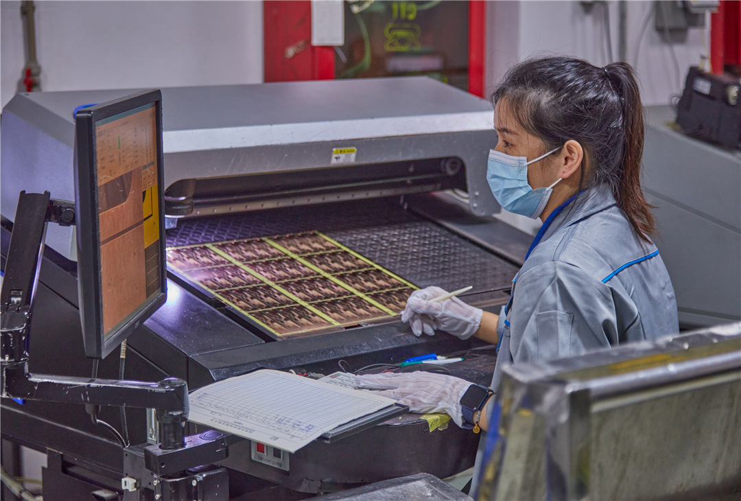
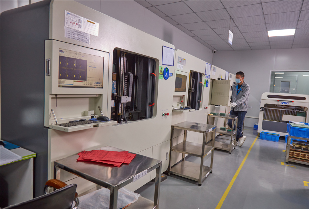
AOI
CCD alignment
Bake Solder Resistance
7. Outer Layer Processing: This process is similar to the inner layer process in the first step and is designed to facilitate subsequent circuit creation.
- Pre-treatment: The board surface is cleaned through pickling, grinding, and drying to enhance dry film adhesion.
- Lamination: A dry film is adhered to the PCB substrate surface in preparation for subsequent image transfer.
- Exposure: UV light exposure causes the dry film on the board to enter a polymerized and unpolymerized state.
- Development: The unpolymerized dry film is dissolved, leaving a gap.
Solder Mask Sandblasting Line
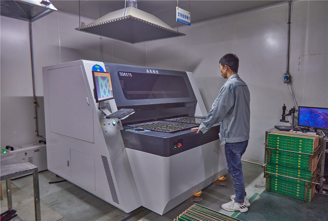
Silkscreen printer
HASL machine
8. Secondary Copper Plating, Etching, AOI
- Secondary Copper Plating: Pattern electroplating and chemical copper application are performed on the areas in the holes not covered by the dry film. This step also involves further enhancing conductivity and copper thickness, followed by tin plating to protect the integrity of the lines and holes during etching.
- Etching: The base copper in the outer dry film (wet film) attachment area is removed through film stripping, etching, and tin stripping processes, completing the outer circuit.
- Outer Layer AOI: Similar to inner layer AOI, AOI optical scanning is used to identify defective locations, which are then repaired by the relevant personnel.
Flying Pin Test
Routing department 1
Route Department 2
9. Solder Mask Application: This step involves applying a solder mask to protect the board and prevent oxidation and other issues.
- Pretreatment: The board undergoes pickling and ultrasonic washing to remove oxides and increase the copper surface's roughness.
- Printing: Solder resist ink is used to cover the areas of the PCB board that do not require soldering, providing protection and insulation.
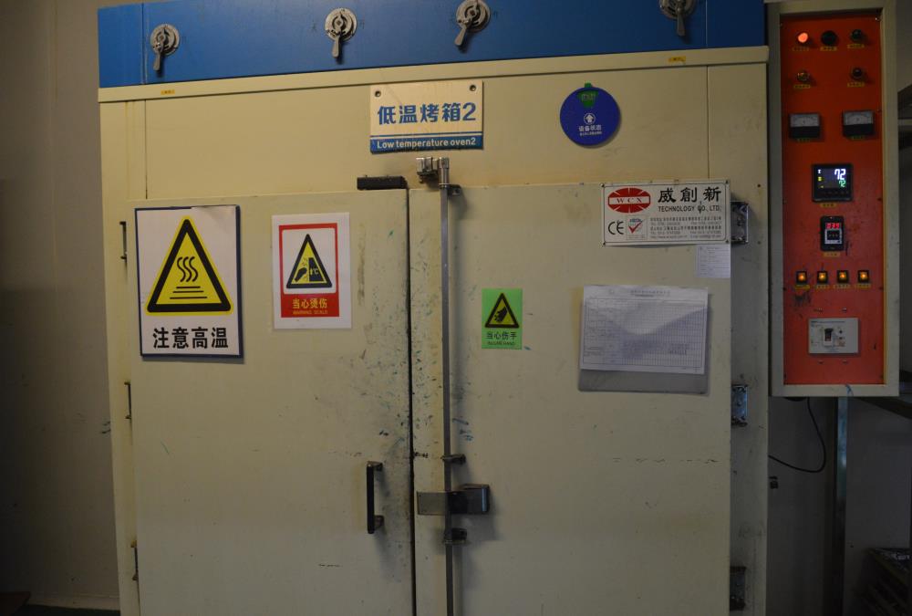
- Pre-baking: The solvent in the solder mask ink is dried, and the ink is hardened in preparation for exposure.
- Exposure: UV light is used to cure the solder mask ink, resulting in the formation of a high molecular polymer through photosensitive polymerization.
- Development: Sodium carbonate solution in the unpolymerized ink is removed.
- Post-baking: The ink is fully hardened.
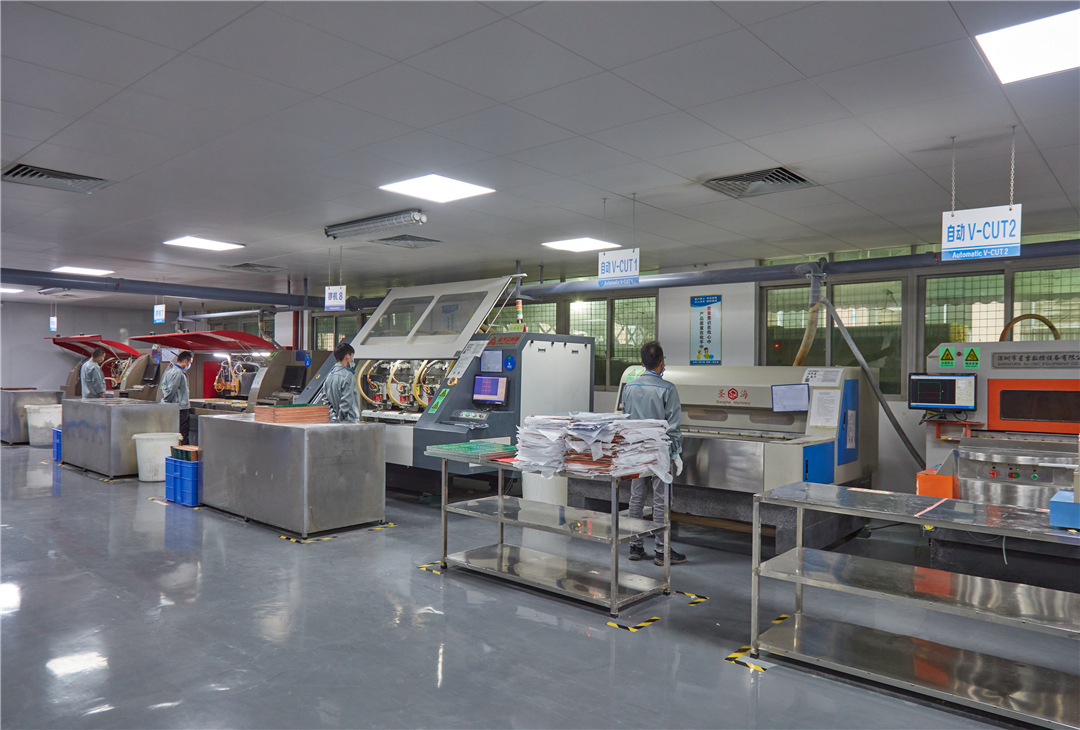
V-cut Machine
Fixture Tooling Test
10. Text Printing: This step involves printing text on the PCB board for easy reference during subsequent soldering processes.
- Pickling: The board surface is cleaned to remove oxidation and enhance the adhesion of the printing ink.
- Text Printing: The desired text is printed to facilitate the subsequent welding processes.
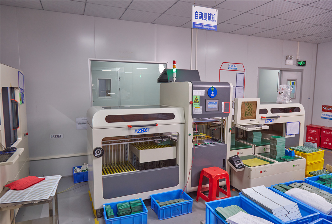
Automatic E-Testing Machine
11.Surface Treatment: The bare copper plate undergoes surface treatment based on customer requirements (such as ENIG, HASL, Silver, Tin, Plating gold, OSP) to prevent rust and oxidation.
12.Board Profile: The board is shaped according to the customer's requirements, facilitating SMT patching and assembly.
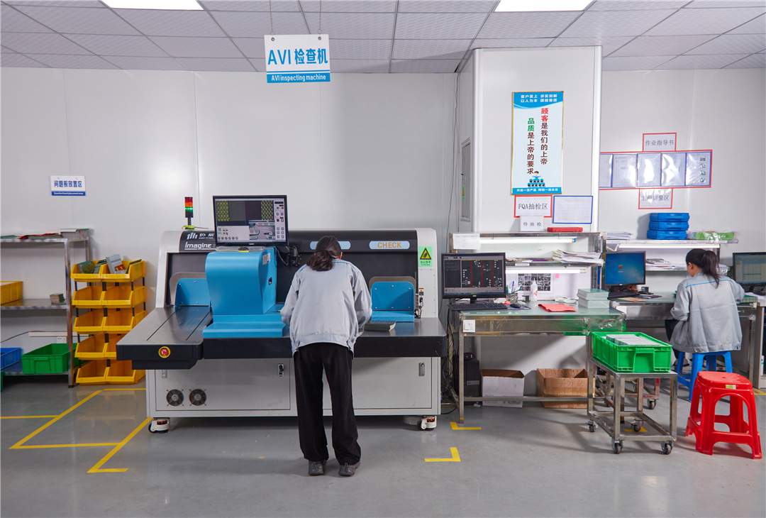
AVI Inspecting Machine
13. Electrical Testing: The board circuit's continuity is tested to identify and prevent any open or short circuits.
14. Final Quality Check (FQC): A comprehensive inspection is conducted after completing all the processes.
Automatic Board-washing Machine
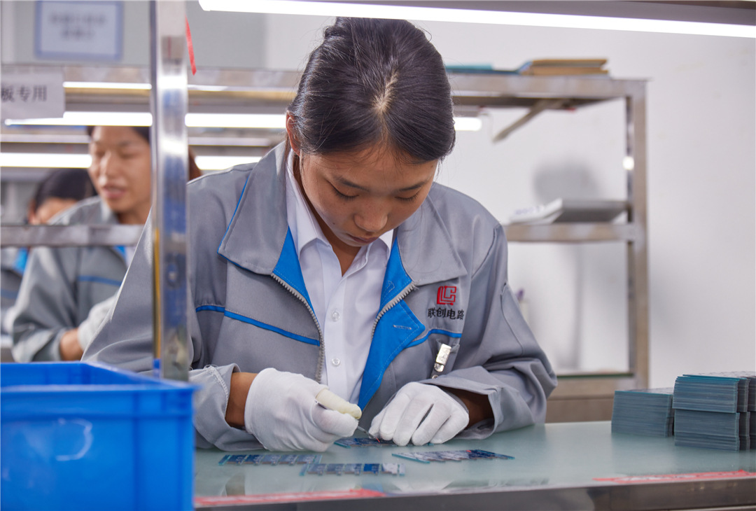
FQC
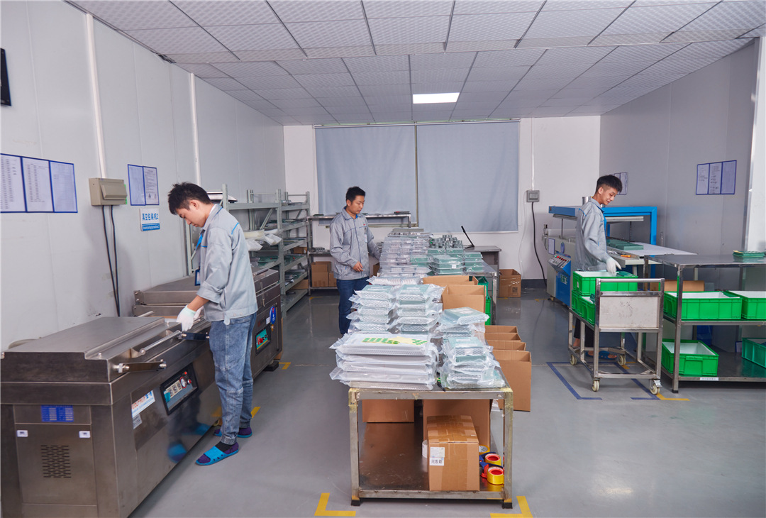
Packaging Department
15. Packaging and Shipment: The completed PCB boards are vacuum-packed, packaged for shipment, and delivered to the customer.