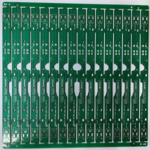
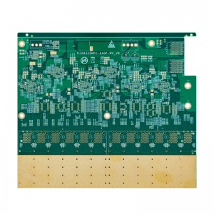
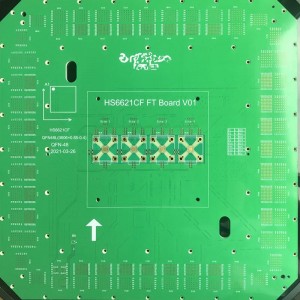
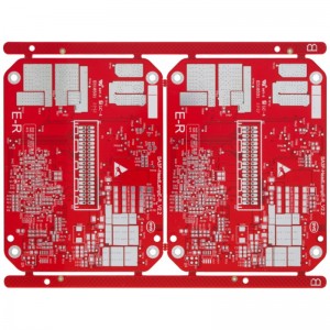
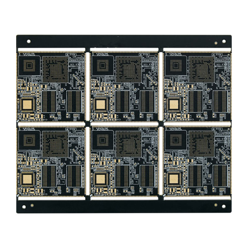
Custom 4-layer Black Soldermask PCB with BGA
Product Specification:
| Base Material: | FR4 TG170+PI |
| PCB Thickness: | Rigid: 1.8+/-10%mm, flex: 0.2+/-0.03mm |
| Layer Count: | 4L |
| Copper Thickness: | 35um/25um/25um/35um |
| Surface Treatment: | ENIG 2U” |
| Solder Mask: | Glossy green |
| Silkscreen: | White |
| Special Process: | Rigid+flex |
Application
At present, BGA technology has been widely used in the computer field (portable computer, supercomputer, military computer, telecommunication computer), communication field (pagers, portable phones, modems), automotive field (various controllers of automobile engines, automobile entertainment products). It is used in a wide variety of passive devices, the most common of which are arrays, networks and connectors. Its specific applications include walkie-talkie, player, digital camera and PDA, etc.
FAQs
BGAs (Ball Grid Arrays) are SMD components with connections on the bottom of the component. Each pin is provided with a solder ball. All connections are distributed in a uniform surface grid or matrix on the component.
BGA boards have more interconnections than normal PCBs, allowing for high-density, smaller sized PCBs. Since the pins are on the underside of the board, the leads are also shorter, yielding better conductivity and faster performance of the device.
BGA components have a property where they will self-align as the solder liquifies and hardens which helps with imperfect placement. The component is then heated to connect the leads to the PCB. A mount can be used to maintain the position of the component if soldering is done by hand.
BGA packages offer higher pin density, lower thermal resistance, and lower inductance than other types of packages. This means more interconnection pins and increased performance at high speeds as compared to dual in-line or flat packages. BGA is not without its disadvantages, though.
The BGA ICs are difficult to inspect because of pins hidden under the package or body of the IC. So the visual inspection is not possible and de-soldering is difficult. The BGA IC solder joint with PCB pad are prone to flexural stress and fatigue that is caused by heating pattern in reflow soldering process.
The Future of BGA Package of PCB
Due to the reasons of cost effectiveness and durability, the BGA packages will be more and more popular in the electrical and electronic product markets in the future. Furthermore, there are a lot of different BGA package types were developed to meet different requirements in the PCB industy, and there are a lot of great advantages by using this technology, so we could really expect a bright future by using the BGA package, if you have the requirement, please feel free to contact us.