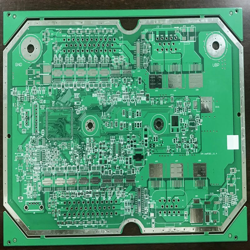
Multi circuit boards middle TG150 8 layers
Product Specification:
| Base Material: | FR4 TG150 |
| PCB Thickness: | 1.6+/-10%mm |
| Layer Count: | 8L |
| Copper Thickness: | 1 oz for all the layers |
| Surface treatment: | HASL-LF |
| Solder mask: | Glossy green |
| Silkscreen: | White |
| Special process : | Standard |
Application
Let's introduce some knowledge of pcb copper thickness.
Copper foil as pcb conductive body, easy adhesion to the insulation layer, corrosion form circuit pattern.The thickness of copper foil is expressed in oz(oz), 1oz=1.4mil, and the average thickness of copper foil is expressed in weight per unit area by the formula: 1oz=28.35g/ FT2(FT2 is square feet, 1 square foot =0.09290304㎡).
International pcb copper foil commonly used thickness: 17.5um, 35um, 50um, 70um. Generally, customers do not make special remarks when making pcb. The copper thickness of single and double sides is generally 35um, that is, 1 amp copper. Of course, some of the more specific boards will use 3OZ, 4OZ, 5OZ... 8OZ, etc., according to product requirements to choose the appropriate copper thickness.
The general copper thickness of single and double sided PCB board is about 35um, and the other copper thickness is 50um and 70um. The surface copper thickness of the multilayer plate is generally 35um, and the inner copper thickness is 17.5um. The use of Pcb board copper thickness mainly depends on the use of PCB and signal voltage, current size, 70% of the circuit board uses 3535um copper foil thickness. Of course, for the current is too large circuit board, copper thickness will also be used 70um, 105um, 140um(very few)
Pcb board use is different, the use of copper thickness is also different. Like common consumer and communications products, use 0.5oz, 1oz, 2oz; For most of the large current, such as high voltage products, power supply board and other products, generally use 3oz or above is thick copper products.
The lamination process of circuit boards is generally as follows:
1. Preparation: Prepare the laminating machine and the required materials (including circuit boards and copper foils to be laminated, pressing plates, etc.).
2. Cleaning treatment: Clean and deoxidize the surface of the circuit board and copper foil to be pressed to ensure good soldering and bonding performance.
3. Lamination: Laminate the copper foil and the circuit board according to the requirements, usually one layer of circuit board and one layer of copper foil are stacked alternately, and finally a multi-layer circuit board is obtained.
4. Positioning and pressing: put the laminated circuit board on the pressing machine, and press the multi-layer circuit board by positioning the pressing plate.
5. Pressing process: Under predetermined time and pressure, the circuit board and copper foil are pressed together by a pressing machine so that they are tightly bonded together.
6. Cooling treatment: Put the pressed circuit board on the cooling platform for cooling treatment, so that it can reach a stable temperature and pressure state.
7.Subsequent processing: Add preservatives to the surface of the circuit board, perform subsequent processing such as drilling, pin insertion, etc., to complete the entire production process of the circuit board.
FAQs
The thickness of the copper layer used usually depends on the current that needs to pass through the PCB. Standard copper thickness is roughly 1.4 to 2.8 mils (1 to 2 oz)
The minimum PCB copper thickness on a copper-clad laminate will be 0.3 oz-0.5oz
Minimum thickness PCB is a term used to describe that the thickness of a printed circuit board is much thinner than normal PCB. The standard thickness of a circuit board is currently 1.5mm. The minimum thickness is 0.2 mm for the majority of circuit boards.
Some of the important characteristics include: fire retardant, dielectric constant, loss factor, tensile strength, shear strength, glass transition temperature, and how much thickness changes with temperature (the Z-axis expansion coefficient).
It is the insulation material that binds the adjacent cores, or a core and a layer, in a PCB stackup. The basic functionalities of prepregs are to bind a core to another core, bind a core to a layer, provide insulation, and protect a multilayer board from short-circuiting.
Products categories
-

Impedance printed circuit boards copper clad pc...
-

Unmanned aerial vehicle PCB quick turn prototyp...
-

Fast turn pcb prototype copper clad pcb board f...
-

Consumer pcb fabrication 94v-0 circuit board di...
-

fast pcb prototyping service quick turn pcb man...
-

Electric vehicle LED PCB quick turn prototype p...