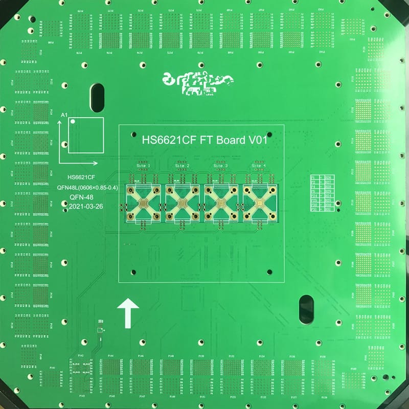
Industrial control PCB FR4 plating gold 26 layers countersink
Product Specification:
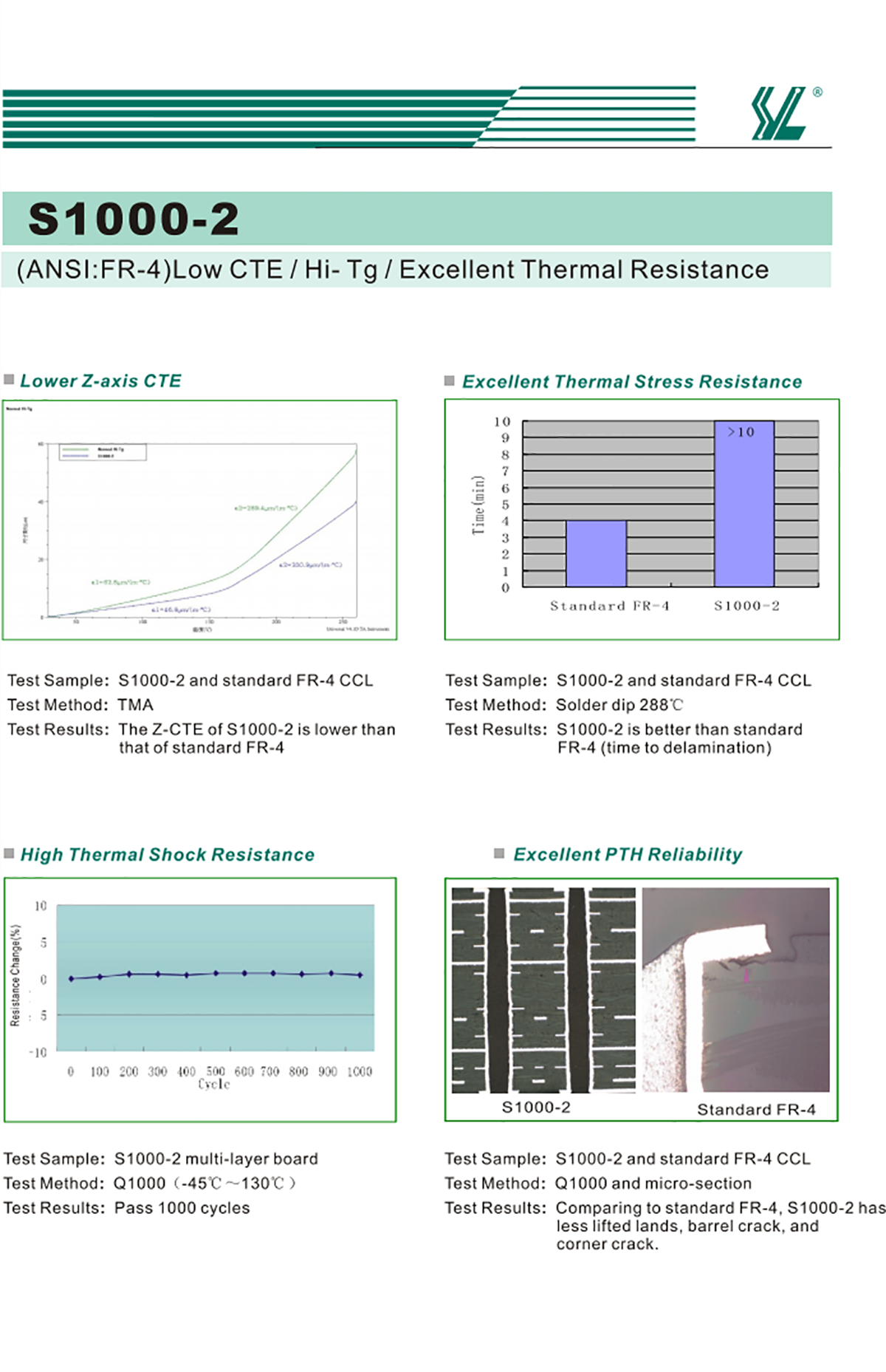
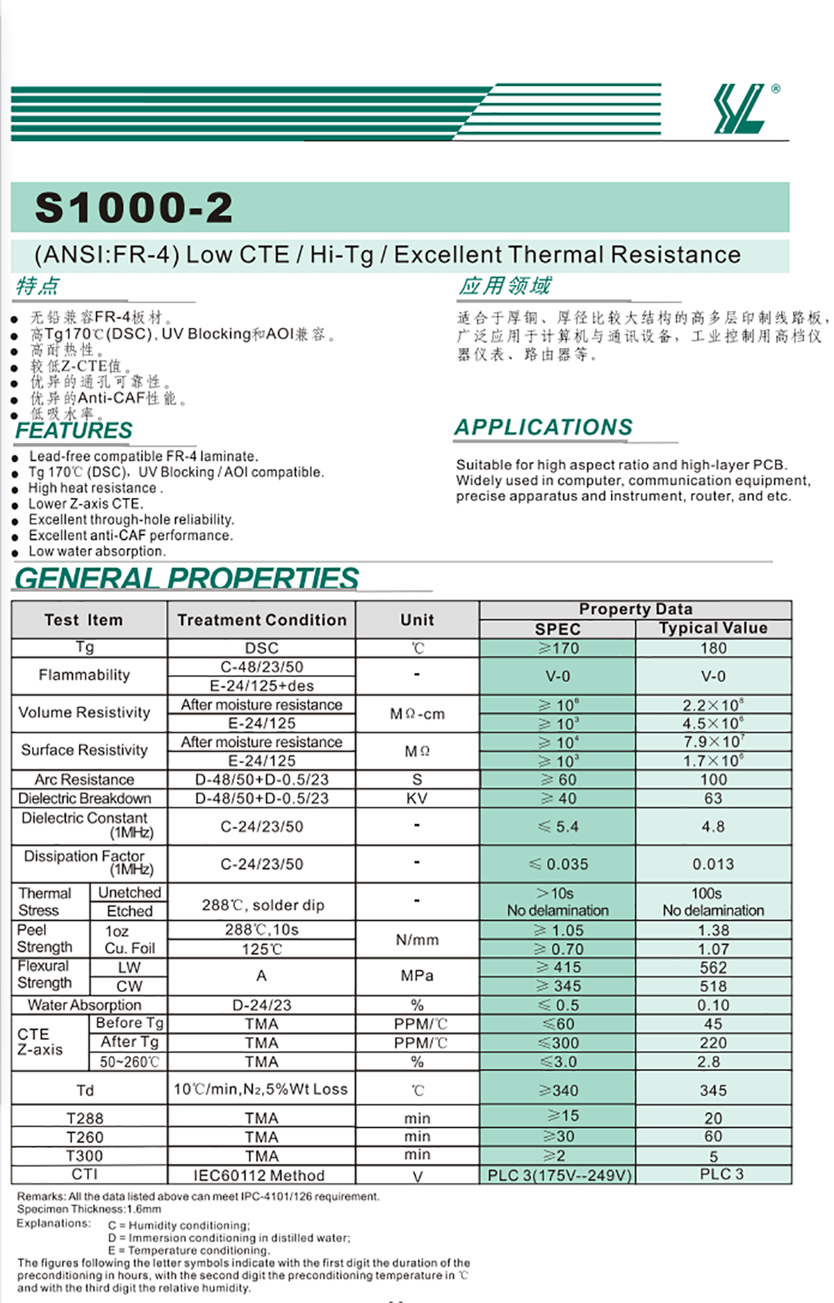
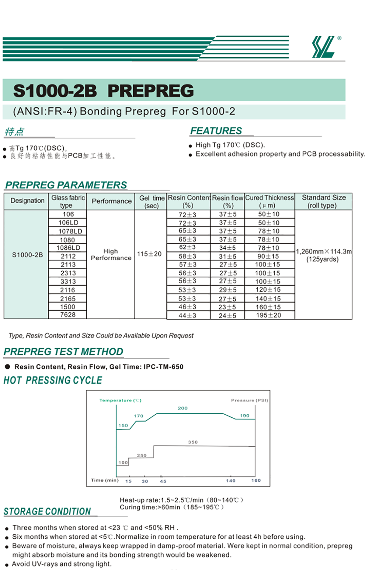
| Base Material: | FR4 TG170 |
| PCB Thickness: | 6.0+/-10%mm |
| Layer Count: | 26L |
| Copper Thickness: | 2 oz for all the layers |
| Surface treatment: | Plating gold 60U” |
| Solder mask: | Glossy green |
| Silkscreen: | White |
| Special process : | Countersink, plating gold, heavy board |
Application
An industrial control PCB is a printed circuit board used in industrial control systems to monitor and control various parameters such as temperature, humidity, pressure, speed, and other process variables. These PCBs are typically ruggedized and designed to withstand harsh industrial environments such as those found in manufacturing plants, chemical plants, and industrial machinery. Industrial control PCBs typically incorporate components such as microprocessors, programmable logic controllers (PLCs), sensors, and actuators that help control and optimize various processes. They may also include communication interfaces such as Ethernet, CAN, or RS-232 for data exchange with other equipment. To ensure high reliability and continuous operation, industrial control PCBs undergo rigorous testing and quality control measures during their design and manufacturing process. They must also comply with industry standards such as UL, CE, and RoHS, among others.
High layers PCB is a printed circuit board with multiple layers of copper traces and electrical components embedded between them. They typically have more than 6 layers and can go up to 50 or more, depending on the complexity of the circuit design. High layers PCBs are useful when designing compact devices that require a large number of components. They help optimize the layout of the circuit board by routing complex tracks and connections through multiple layers. This results in a more compact and efficient design that saves space on the board. These boards are typically used in high-end electronics applications, such as aerospace, defense, and telecommunications industries. They require advanced manufacturing techniques, such as laser drilling and controlled impedance routing, to ensure high precision and reliability. Due to their complexity, designing and manufacturing high layers PCBs can be more expensive and time-consuming than standard PCBs. Additionally, the more layers a PCB has, the higher the probability of errors during design and manufacturing. As a result, high layers PCBs require extensive testing and quality control measures to ensure their functionality and reliability.
Countersink a PCB refers to the process of drilling a hole in the board and then using a larger diameter bit to create a conical recess around the hole. This is often done when the head of a screw or bolt needs to be flush with the surface of the PCB. Countersink is typically done during the drilling stage of PCB manufacturing, after the copper layers have been etched and before the board has been through the solder mask and silkscreen printing process. The size and shape of the counter-sunk hole will depend on the screw or bolt being used and the thickness and material of the PCB. It's important to ensure that the countersink depth and diameter are appropriate to avoid damaging the components or traces on the PCB. Countersink a PCB can be a useful technique when designing products that require a clean and flat surface. It allows screws and bolts to sit flush with the board, creating a more aesthetically pleasing appearance and preventing snagging or damage from protruding fasteners.
FAQs
Plating gold is a type of PCB surface finish, also known as nickel gold electroplating. In the PCB manufacturing process, plating gold is to deposit a layer of gold plated over a barrier coat of nickel by electroplating. Plating gold can be divided into ''hard gold plating'' and ''soft gold plating''.
Frequently used in combination with nickel plating, the thin layer of gold protects the component from corrosion, heat, wear and helps ensure a reliable electrical connection.
Hard gold plating is a gold electrodeposit that has been alloyed with another element to alter the grain structure of the gold. Soft gold plating is the highest purity gold electrodeposit; it is essentially pure gold without the addition of any alloying elements
A countersink hole is a cone-shaped hole that is notched or drilled into a PCB laminate. This tapered hole allows a flat-head socket screw head to be inserted in the drilled hole. Countersinks are designed to allow the bolt or screw to stay tucked inside with a planarized board surface.
82degrees, 90degrees and 100degrees
Products categories
-

Automobile lamp PCB china pcb supplier double s...
-

Fast turn circuit board manufacturing custom do...
-

Electric car prototype printed circuit board ma...
-

Pcb processing prototype board 94v-0 Halogen-fr...
-

Quickturn pcb tg 150 degrees green soldermask q...
-

Fast turn pcb prototype copper clad pcb board f...