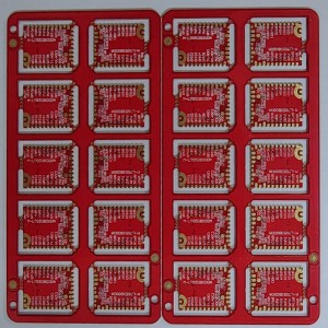
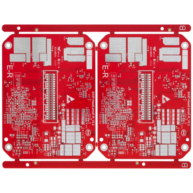
Custom 2-layer rigid PCB with red solder mask
Product Specification:
| Base Material: | FR4 TG130 |
| PCB Thickness: | 1.6+/-10%mm |
| Layer Count: | 2L |
| Copper Thickness: | 35um/35um |
| Surface Treatment: | HASL lead free |
| Solder Mask: | Red |
| Silkscreen: | White |
| Special Process: | None |
Application
Double-sided circuit board is mainly to solve the circuit complex design and area limitations, on both sides of the board installed components, double-layer or multi-layer wiring.Double-sided PCBs are often used in vending machines, cellphones, UPS systems, amplifiers, lighting systems, and car dashboards. Double-sided PCBs are best for higher technology applications, compact electronic circuits, and complex circuits. Its application is extremely wide and the cost is low.
FAQs
The 2-layer PCB is copper coated on both sides with an insulating layer in the middle. It has components on both sides of the board, which is why it is also called a double-sided PCB. They are fabricated by joining two layers of copper together, with a dielectric material in between.
You can surmise what the apparent difference is between the 2 layers PCB and 4 layers PCB according to their names. 2 layers PCB has two sided traces with a top and bottom layer, while 4 layers PCB has 4 layers. If you have a better understanding of two types of PCB boards, you will find that there are many differences in how they are constructed and how to work.
Single-sided PCB traces are present on only one side, while double-sided PCBs have traces on both sides with top and bottom layers. The components and conductive copper are mounted on both sides of a double-sided PCB, and this leads to the intersection or overlap of the trace.
Yes, just send us your gerber file.
3WDS.
The 2 layer PCB ( double-sided PCB )is a printed circuit board with copper coated on both sides, top and bottom. There is an insulating layer in the middle, which is a commonly used printed circuit board. Both sides can be layout and soldered, which greatly reduces the difficulty of layout, so it is widely used.
To use circuits on both sides, there must be a proper circuit connection between the two sides. The “bridges” between such circuits are called vias. A via is a small hole on the PCB board filled or coated with metal, which can be connected with the circuits on both sides. Because the area of the double-sided board is twice as large as that of the single-sided board, the double-sided board solves the difficulty of the single-sided board due to the interlaced layout (it can be connected to the other side through the holes), and it is more suitable for more complicated circuits than the single-sided board.
We need electronic products with high performance, small size, and multiple functions, which promotes the development of printed circuit board manufacturing to be light, thin, short, and small. With limited space, more functions can be realized, layout density has become greater, and the hole diameter is smaller. The minimum hole diameter of mechanical drilling capacity has dropped from 0.4mm to 0.2mm or even smaller. The hole diameter of the PTH is getting smaller and smaller. The quality of the PTH (Plated Through Hole) on which the layer-to-layer interconnection depends is directly related to the reliability of the printed circuit board.